深圳市的美科技有限公司\\
主营产品:
深圳市的美科技有限公司\\
主营产品:
2023年07月20日 19:45
功能 |
绝缘装置陶瓷 |
规格尺寸 |
多种(mm)mm(mm) |
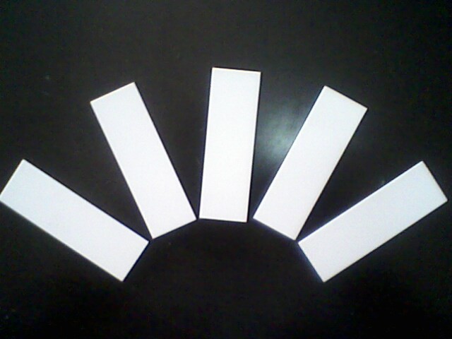
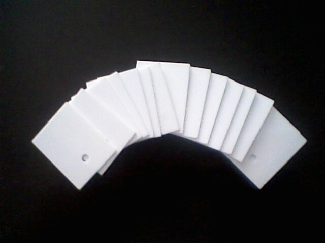
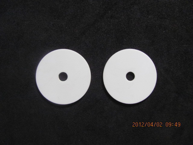
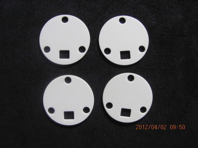
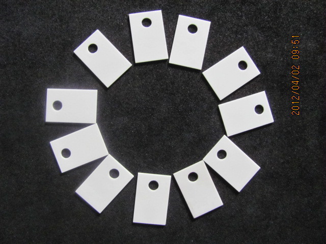
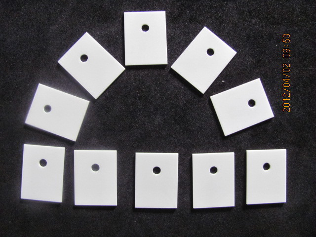
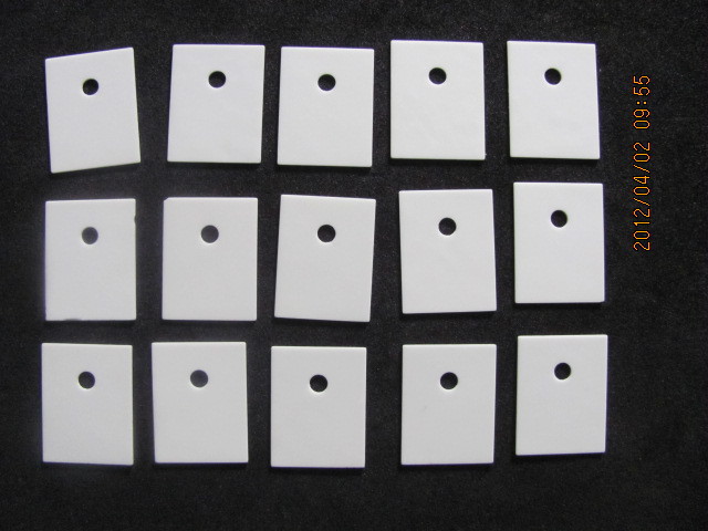
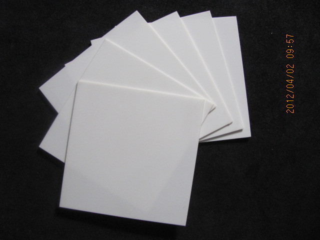
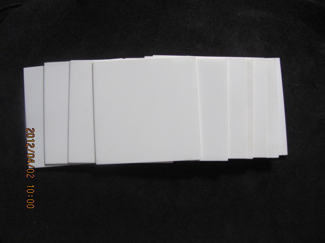
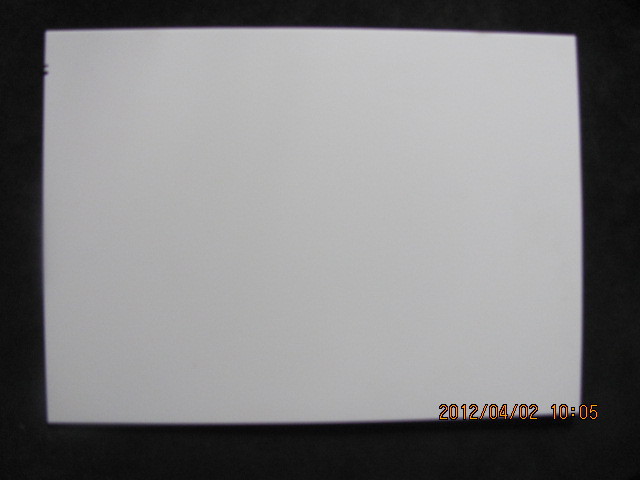
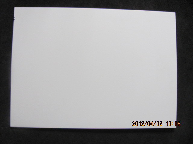
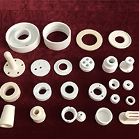
深圳市的美科技电子有限公司一般采用流延成型法制备氧化铝陶瓷基片,目前发展到使用非苯系、无毒、无公害溶剂体系,对环境无污染,且流延坯片的干燥速率易于控制,配料中使用的溶剂可回收循环利用。在流延生坯上可以冲制各种形状和孔,然后进行烧成,可在连续式空气气氛窑炉中同时完成排胶和烧成的生产方式。96%氧化铝陶瓷基片材料中添加了合适的矿物原料作为助熔剂,烧成温度低到1580℃~1600℃,产品密度即可达3.75g/cm3以上。对于尺寸精度要求较高的产品,可以在烧成后,以激光加工方法,在基片上划线、打孔,精度达到±0.05mm。
Ceramic substrate, also called ceramic substrates, electronic ceramic substrate is for, to film circuit components and the appropriate elements to form a support base, sheet material. ording to the different of the application of ceramic substrate, and pided into HIC (hybrid integrated circuit) ceramic substrate, the focus potentiometer ceramic substrate, the laser heating fuser ceramic substrate, the chip resistor substrate, the network resistors substrate, etc.; ording to the different methods of processing, ceramic substrate is pided into moulding piece, laser crossed piece two kinds big. Moulded piece of
The main features of high-temperature ceramic substrate, electric insulation performance is high, dielectric constant and medium loss, low thermal conductivity, good stability, and chemical components such as thermal expansion coefficient of similar major advantages, but brittle ceramic substrate, the area more ? made substrate
The main features
Ceramic substrate with high temperature, electric insulation performance is high, dielectric constant and medium loss, low thermal conductivity, good stability, and chemical components such as thermal expansion coefficient of similar major advantages, but brittle ceramic substrate, made of substrate area is lesser, high cost.
Development direction
Along with the progress of the microelectronics technology, the processing technology of the characteristic line width has reached a sub-micron, a piece of substrate can be integrated 106 ~ 109 more elements, circuit to work faster and faster, higher frequency, the substrate materials performance put forward higher request. As a hybrid integrated circuit cracking (HIC) and multichip module (MCM) one of the key materials, boards of its total cost of about 60%. Ceramic substrates development direction is always low dielectric often ?
The beauty of shenzhen science and technology electronic ceramics Co., LTD. General use of the flow ChengXingFa alumina ceramic substrate delay preparation, the present development to use the benzene department, non-toxic, pollution-free solvent systems, free from pollution to the environment, and the flow of billet delay the drying rate of easy to control, ingredients used in solvent recovery recycling. In the flow can be blunt the green delay of various shapes and hole, then firing, can be in the continuous air atmosphere in kiln finish at the same time row glue and firing mode of production. 96% alumina ceramic substrate materials added to the mineral right as raw material flux, firing temperature to 1580℃~ 1600 low℃, the product can reach 3.75 g density/cm3 above. For size higher uracy of products, can be in
联系方式