广州从谊计算机有限公司
主营产品:
13543425800
广州从谊计算机有限公司
主营产品:
2023年10月05日 12:37
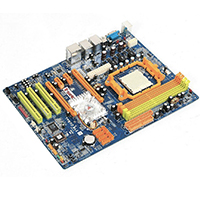
内存类型 |
DDR |
适用类型 |
台式机 |
插脚数目 |
240Pin |
颗粒封装 |
FBGA |
品牌/型号 |
金士顿/KHX2000C9AD3T1K3/6GX |
KHX2000C9AD3T1K3/6GX 6GB (2GB 256M x 64-Bit x 3 pcs.) DDR3-2000MHz CL9 240-Pin DIMM Kit DESCRIPTION: Kingston's KHX2000C9AD3T1K3/6GX is a kit of three 256M x 64-bit 2GB (2048MB) DDR3-2000MHz CL9 SDRAM (Synchronous DRAM) memory modules, based on sixteen 128M x 8-bit DDR3 FBGA components per module. Each ? XMP (Extreme Memory Profiles). Total kit capacity is 6GB. Each module kit has been tested module kit supports Intel to run at DDR3-2000MHz at a low latency timing of 9-10-9-27 at 1.65V. The SPDs are programmed to JEDEC standard latency DDR3-1333MHz timing of 9-9-9 at 1.5V. Each 240-pin DIMM uses gold contact fingers and requires 1.5V. The JEDEC standard electrical and mechanical specifications are as follows: FEATURES: JEDEC standard 1.5V !à 0.075V Power Suppl VDDQ = 1.5V !à 0.075 Keyed 667MHz fCK for 1333Mb/sec/pin Keyed 8 independent internal bank Keyed Programmable CAS Latency: 5,6,7,8,9,10 Posted CAS Programmable Additive Latency: 0, CL - 2, or CL - 1 clock Programmable CAS Write Latency(CWL) = 7(DDR3-1333) 8-bit pre-fetch Burst Length: 8 (Interleave without any limit, sequential with starting address !°000!± only), 4 with tCCD = which does not allow seamless read or write [either on the fly using A12 or MRS] Bi-directional Differential Data Strobe Internal(self) calibration : Internal self calibration through ZQ pin (RZQ : 240 ohm !à 1% On Die Termination using ODT pin Average Refresh Period 7.8us at lower then TCASE 85!aC, 3.9us at 85!aC < TCASE . 95 Asynchronous Reset PCB : Height 2.401!± (61.00mm) w/ heatsink, double sided componen PERFORMANCE: CL(IDD)9 cycles Row Cycle Time (tRCmin)49.5ns (min.) Refresh to Active/Refresh Command Time (tRFCmin) 110ns Row Active Time (tRASmin)36ns (min.) Power1.800 W (operating per module) UL Rating94 V - 0 o o Operating Temperature0 C to 85 C o o Storage Temperature-55 C to 100 C Document No. 4805509-001.B00 Page 1 04/21/10

联系方式